
COMPASS - Virtual - November 2021
ARCHIVE VIEW
This event has already occurred
Return to COMPASS main page
AGENDA
Presentation videos will be available shortly. For access please complete the request form below.
Executive Welcome and Roadmap (FormFactor Inc.)
Executive Welcome and Roadmap

Amy Leong, Chief Marketing Officer and Senior Vice President, M&A, General Manager
Amy Leong has served as our Chief Marketing Officer since 2017 with added responsibilities as our Senior Vice President, M&A and General Manager of the Emerging Growth Business Unit since 2020. Prior to FormFactor, Amy held the position of VP of Marketing at MicroProbe from 2010 through the October 2012 closing of FormFactor’s acquisition of MicroProbe. Before joining MicroProbe, Amy worked at Gartner, Inc. as a Research Director from 2008 to 2010 and covered the foundry & logic market and various emerging applications. From 2003 to 2008, Amy worked at FormFactor where she served as Senior Director of Corporate Strategic Marketing and Director of DRAM Product Marketing. Prior to FormFactor, she worked in a variety of semiconductor process engineering, metrology, and product marketing roles at KLA and IBM. Amy holds an M.S. in Material Science and Engineering from Stanford University and a B.S. in Chemical Engineering from the University of California, Berkeley.
Keynote: Path to a Useful Quantum Computer” (PsiQuantum)
Keynote: “Path to a Useful Quantum Computer”

Mark Thompson, Chief Technologist, PsiQuantum
Mark Thompson is Co-Founder and Chief Technologist of PsiQuantum. He has over 20 years' experience in the fields of photonics and quantum technologies, with a PhD from Cambridge University, industrial positions at Toshiba, Corning, Bookham Technology, PsiQuantum, a Professorship at the University of Bristol and Fellowship at the University of Cambridge. He established the Bristol Centre for Quantum Engineering and the Bristol Quantum Technology Enterprise Center, and has held prestigious UK and European fellowships and prizes. He has more than 100 publications and patents and has founded two startup companies in quantum technologies.
Customer Presentation: "Characterization of 1/f noise at wafer level, using CM300xi-ULN" (STMicroeletronics)
Customer Presentation: Characterization of 1/f noise at wafer level, using CM300xi-ULN
An investigation of differences, in term of noise performances, detected in a product transferred from a technology to another one, has been conducted on 1.8V n-ch MOS transistor,130nm lithography. The 1/f characterization has been carried out at different overdrive values as low as Vgs-Vth close to zero reaching low noise levels typically undetectable on standard probe stations. The fastest way to do it is to perform measurements at wafer level. CM300x-ULN becomes the suitable probing system, thanks to the completely shielded microchamber, filtered power line, and the positioning of the system after a deep and extensive environment including floor vibration evaluation, AC power line noise and harmonics, low frequency magnetic field strength.

Lorenzo Labate, Characterization & Modeling Project Manager, STMicroeletronics
Lorenzo Labate was born in Abbiategrasso (Milan), Italy, in 1969. He received the diploma degree in industrial electronics from Technical Industrial Institute “E. Alessandrini” of Abbiategrasso. Since 1990 he has been with STMicroelectronics, Milan, Italy, and in the Technology R&D group fully devoted to components electrical characterization of BCD technologies. In particular for characterization of NVM embedded in a mixed technology. He fully participates to the developing of very first MEMS accelerometers and consequent characterization. Furthermore, he was involved to develop of RF LDMOS transistor, including set up of a load-pull system, characterization, and modeling at RF large signal. He participates to SOI devices modeling, including self-heating effects, HV (600V/1200V) MOS transistors, integrated JFET, galvanic isolators, HV (10V/200V) MOS transistors in smaller lithography. Last but not least he has the responsibility of electrical characterization lab of Smart Power Technology R&D division.
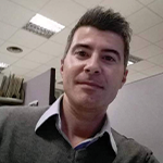
Fausto Simioni, STMicroeletronics
Fausto Simioni was born in Vigevano (Pavia), Italy, in 1976. He received the bachelor’s degree in electronics engineering from University Of Pavia. Since 1998 he has been with STMicroelectronics, Milan, Italy, and in the Technology R&D group, in the beginning as part of the newly created EMC Laboratory, dedicated to performing EMC characterization of automotive microcontrollers, MEMS accelerometers and memories. In 2006 he internally moved to the BCD Modeling And Characterization group, focusing in particular on the characterization and modeling of BJT, resistors and zener diodes across various technologies, formerly performing also SOA characterization of power MOS. Among the other activities, he is now in charge of performing noise 1/f characterization and modeling of MOS, BJT and resistors, an activity which, across the years, is becoming more and more relevant.
Technical Presentation: "mmW Test Solutions for 5G-FR2" (FormFactor Inc.)
Technical Presentation: mW Test Solutions for 5G-FR2
5G-FR2 is pushing the boundary of RF test in production environments. In particular, the increase in chip complexity is requiring more channels in a single chip, as well as pushing the requirements for parallel test. In order to do this, increasing the density of I/O has required the development of not only larger probing solutions, but higher routing density. I will talk about the larger probe card solutions, looking at the increase of routing with additional routing layers, as well as signal integrity to show that increases in channel count doesn’t necessarily require giving up on mW test capabilities in high volume manufacturing environments.

Daniel Bock, RF Applications Engineer, FormFactor Inc.
Daniel Bock got his Ph.D. in Physics at Carnegie Mellon University in 2006, working on Superconducting Nanowire Bolometers in the NanoFabrication Lab. He then went to work in 2007 with Physical Optics Corporation in Torrance, CA. There, he was awarded more than $4M in SBIR research grants from the Department of Defense, developing innovative high power tunable filters for use in Electronics Warfare and Electronics Attack systems. He joined the Cascade Microtech Business Unit in June of 2012. Since joining, he has been working to extend the mmWave bandwidth of Pyramid Probe technology, including RF test of automotive radar devices. He has also led the development of the Custom Calibration Substrate (Custom ISS) product line to supplement the standard ISS line.
Technical Presentation: "Too hot to test for leading-edge SoC and heterogenous integrated IC stack" (ATT Systems)
Technical Presentation: Too hot to test for leading-edge SoC and heterogenous integrated IC stack
Leading-edge AI/Graphic/mobile processors, DRAM devices, and heterogenous integrated IC stacks are all facing the same set of thermal management challenge -- DUT is too hot to test. Even at room temperature wafer chuck setting, a mobile SoC device junction temperature can get well above 100 to 150C. For DRAM full-wafer testing, 1-2K watts of power could be applied during 1-TD testing, posting challenges for test cell thermal management. This results in inaccurate test results, or frequently burned probes which cause test cell downtime. As the heterogenous integration becomes more popular, the thermal challenges to test the base die with multi-chips stacked on top further exuberate as the thermal loading per silicon area can increase by order of magnitude. You can’t improve what you can’t measure. FormFactor latest low-thermal-resistance (LTR) wafer chuck technology applies multiple temperature sensors to accurately detect DUT temperature and adjust heat dissipation to achieve the desired test temperature. LTR has shown promising results in production test to address the “too hot to test” challenge.
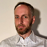
Ferdinand Wimmer, Electrical Engineer, ATT Systems GmbH/ FormFactor Inc.
Ferdinand Wimmer has worked at ATT Systems since 2005 as an Electrical Engineer. The focus of his work is product development from the chuck up to the cooling units. He is also responsible for software development for ATT’s chuck systems. He acquired a degree in Electrical Engineering at the University of Applied Sciences Deggendorf (Germany).
Partner Presentation: "Efficient Wafer & Chip Test" (Keysight Technologies}
Partner Presentation: Efficient Wafer & Chip Test - (Keysight Technologies)
Integrated photonic devices require comprehensive testing for optical and electro-optical parameters at the wafer or chip level. Keysight’s integrated photonics test solution supports the workflow from chip design to test and analytics through easily configurable test scripts which include calibration and de-embedding of optical and RF paths between instruments and the DUT. Optical tests are possible in the full 1260 to 1650 nm range through new C-series optical instruments. Electro-optical tests ranging from DC to 110 GHz are made with a N4372E lightwave component analyzer paired with M9601A and M9615A modular source measure units.

Dr.-Ing. Hansjoerg Haisch, Program Manager, Integrated Photonics Test Solutions, Keysight Technologies
Dr. HansJoerg Haisch is responsible for definition and development of Integrated and Silicon Photonics test solutions covering optical and electro-optical parametric test in wavelength, DC, frequency and time domain up to above 110 GHz, including solution calibration and verification methods and services for Keysight. Prior to this role, he was R&D Manager Photonic Measurement Solutions and responsible for R&D of Photonic Measurement Solutions in the Digital Photonic Test Division of Keysight Technologies. Hansjoerg was also an R&B operating manager at Agilent Technologies for over 12 years.
Technical Presentation: "FRT Metrology for Advanced Packaging" (FormFactor Inc.)
Technical Presentation: FRT Metrology for Advanced Packaging
Advanced packages have enabled the industry to develop new flip-chip processes, 2.5D interposer and TSV technology, and most recently, 2D and 3D fan-out processes with high densities of connections in the smallest of spaces. With advanced packaging, the need for flexibility in wafer metrology and handling has just exploded. Our FRT MicroProf® AP system is specifically designed for metrology advanced packaging applications.
FRT MicroProf® AP measures and handles numerous wafer types up to 12 inches for both front and back end: bare, structured, coated, bonded, highly warped, thinned, TAIKO and fan-out wafers, even wafers with Micro-Electronic-Mechanical components or at different 3D packaging process steps, but also glass, lens, and non-SEMI-standard wafers, panels and film frames.
With our SurfaceSens multi-sensor technology, the modular based software and the retrofittable sensor hardware we create the flexibility customers need in heterogeneous production cycles.
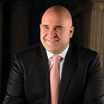
Kenan Goerguelue, Head of Sales & Business Development, FRT Division, FormFactor, Inc.
Kenan Görgülü is Head of Sales & Business Development for the FRT Division of FormFactor with responsibility for the global sales & business development organization across all corporate sales sites in EMEA, Americas and Asia Pacific. Prior to joining FormFactor, he was regional sales director at Sartorius, a supplier to the life science research and the biopharmaceutical industry.
He holds an MBA from the International School of Management and a degree in mechanical engineering from Middle East Technical University/Erciyes University.
Technical Presentation: "Probe Card Solutions to Address Leading Edge Advanced Package Test Requirements" (FormFactor Inc.)
Technical Presentation: Probe Card Solutions to Address Leading Edge Advanced Package Test Requirements
Recent industry wide adoption of heterogeneous integrated systems enabled by 2.5D and 3D advanced packaging technology is driving up the demand and technical challenge on testing. The complexity of advanced packaging has increased dramatically, challenging packaging cost and package yield.
In the wafer testing area, test requirements are moving in the direction of high speed, high current carrying capacity and wider temperature range in both Memory and SoC wafer test. in this paper we will share recent production developments and solutions to meet leading edge testing requirements in High Bandwidth Memory and SoC ICs as part of advanced packaging.
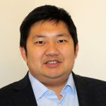
Alan Liao, Director of Product Marketing, FormFactor, Inc.
Alan Liao has been with FormFactor since August 2008. As an electrical design engineer he designed the first 300mm full wafer contact probe card for SmartPhone DRAM wafer sort testing. Alan also participated as electrical R&D engineer to continuously improve and develop Probe Card technology meets advance memory testing requirement. In 2012, Alan moved to the customer design engineer position to be the technical interface with key north America DRAM customers. During 2014, Alan joined product marketing as an SoC product manager. In 2019 he was promoted to Director of probe Business Unit product marketing response to the Asia region product Marketing.
Mr. Liao holds an M.S. in Analog Circuit Design and Analysis from Silicon Valley University (SJSU) and a B.S. in Electrical Engineering from the University of California, Los Angeles (UCLA).
VIDEO REQUEST FORM
Keynote: “Path to a Useful Quantum Computer”

Mark Thompson, Chief Technologist, PsiQuantum
Mark Thompson is Co-Founder and Chief Technologist of PsiQuantum. He has over 20 years' experience in the fields of photonics and quantum technologies, with a PhD from Cambridge University, industrial positions at Toshiba, Corning, Bookham Technology, PsiQuantum, a Professorship at the University of Bristol and Fellowship at the University of Cambridge. He established the Bristol Centre for Quantum Engineering and the Bristol Quantum Technology Enterprise Center, and has held prestigious UK and European fellowships and prizes. He has more than 100 publications and patents and has founded two startup companies in quantum technologies.
