About COMPASS
The 2023 COMPASS Theme is Megatrends in Test and Measurement
FormFactor’s COMPASS test and measurement community event brings together FormFactor customers from around the
world to discuss the products and technologies shaping our future. Industry leaders and speakers from corporations,
leading-edge research institutions and FormFactor share test insights on a wide variety of emerging applications
including 5G, trends in advanced packages, next generation memories and other devices, ultra-low noise testing,
cryogenic probing and millimeter-wave measurement and calibration.
Thank You COMPASS 2023 Participants!
KEYNOTE SPEAKER
Advanced Packaging:
Enabling Moore’s Law’s Next Frontier
Dr. Deepak Kulkarni
FELLOW, ADVANCED PACKAGING, AMD

Agenda
Welcome & Executive Address
Mike Slessor, President & CEO - FormFactor Inc.
Keynote Presentation - Advanced Packaging: Enabling Moore’s Law’s Next Frontier
Dr. Deepak Kulkarni, Fellow, Advanced Packaging, AMD
Chiplet architectures are fundamental to the continued economic viable growth of power efficient computing. Thus, the criticality of advanced packaging technologies and architectures correlated to Moore’s Law’s next frontier is high. New heterogeneous architectures, along with AMD’s industry leading advanced packaging roadmap, enable power, performance, area, and cost (PPAC). PPAC considerations per product influence the choice of Substrate (2D), Fanout based (2.5D) and Hybrid Bonded (3D) technologies and will be addressed in this keynote. Finally, AMD’s High Performance Fanout previewed in the RDNA3 architecture along with enabling technologies like power delivery and thermal improvements will be detailed.
Pyramid Probe: RF Calibration and Probe Aging Considerations in HVM High Speed IO Devices
Pratik Ghate, Principal RF Engineer, FormFactor Inc.
The growth in AI (such as ChatGPT and BING AI) is requiring large investments into the expansion of data centers, driving higher and higher data rates in IO devices. In order to reach these data rates, wafer test is moving to bandwidth > 60 GHz. Pyramid Probes are widely used for wafer test at up to 81 GHz and in high volume manufacturing (HVM). These probes feature micro-strip or CPW transmission lines that provide controlled impedance and low loss (<6 dB at 67 GHz) for the industry leading performance at wafer test. However, in the standard layout, the signal trace faces the wafer and is only 70 um away, so that it can sometimes couple to structures on the wafer. This coupling can have significant effects in some cases, in both DUT performance and RF calibration of the probe head. Further, one expects the coupling to increase as the probe ages and the tips become shorter, bringing the microstrip closer to the wafer. To reduce this coupling, Pyramid Probes using a microstrip with the ground between the transmission line and the wafer (inverted microstrip) are available. In this study, we will use probes with standard and inverted microstrips to measure TIA (transimpedance amplifier) performance. Measurements before and after aging the probes will be compared to characterize these effects. In addition, we will look at different calibration methods (SOLR, SOLT, SOL de-embed) and compare them to provide recommendations for calibration.
How FormFactor’s Known Good Die Test Enables Advanced Packaging for High Bandwidth Memory – Solutions and Latest Trends
David Cooke, Product Marketing Manager, FormFactor, Inc.
The need for high bandwidth computing has driven the development of 3D Heterogenous modules, these vertically stacked memory packages for High Bandwidth Memory have many benefits over traditional modules, lower power consumption, significantly higher memory storage, higher performance coupled with smaller and smaller footprints.
Advanced packaging IC revenues continue to grow year on year. The advent of this technology has created the need for known good die test of the TSV connected memory stacks to reduce risk and cost. Early test data on the stack yield after manufacturing is essential to control final costs. FormFactor probe solutions provide the necessary test medium for aluminum pads for sort and functional speed test using FFI’s T11 family of probes and copper bumps with vertical MEMs MF family.
In this presentation we will explore how we engage in this market.
Pharos Vertical and Edge Coupling Low Loss SiPh Wafer Test with Fully Automated Calibration - From Probe Install to Successful V-groove Wafer Level Test in 90 Minutes
Simon Reissmann, Sr. Principal Applications Engineer, FormFactor, Inc.
In this talk we will discuss FormFactor’s industry leading silicon photonics coupling technology, Pharos, for edge coupling in V grooves and lowest loss coupling on grating couplers. Further we will cover the new four mouse-click automated calibration routine released in the latest silicon photonics software solution suite.
FormFactor’s SiPh solution includes a built-in power measuring function that quantifies the laser output coming directly from one of the Pharos fiber channels. This allows the user the flexibility to move from measurements directly on the wafer to an aux site and verify the laser power coming out of the probes, automatically position one of the eight channels of the probes, and to go back to the last die or subdie measured to proceed. All that is accomplished by sending one integrated command, without the need to manually navigate to the right spot on the aux site, position the probe in the correct location, and so on. This eliminates user miscues completely and is a great timesaver.
Also, with a four mouse-click automated calibration, manual errors are eliminated. This automated routine assures consistent and repeatable calibration results without missing a step, and saves significant time.
Measuring Superconducting Material Properties for Cryogenic Chip Development
Brandon Boiko, Sr. Applications Engineer, FormFactor Inc.
Many emerging technologies in Quantum and High-Performance Computing industries rely on the use of superconducting materials and their unique properties. Components like SNSPDs and SQUIDs use common superconductors like Nb and Al for their convenient transition temperatures of ~10K and ~1K respectively. Development of new exotic superconductors with better performance and manufacturability is an ongoing area of research. This talk will discuss the general measurement methodologies and best practices for characterizing the transition temperature for superconducting materials.
Maximizing CCC in a Probe Card and the March to an Unburnable Probe
Hadi Najar, Sr Principal Engineer Mechanical Design, FormFactor, Inc.
Datacenters and High-Performance-Compute (HPC) applications are quickly approaching and even exceeding 1kW of total power in a single chip in normal operating conditions. In addition to new applications, the transition to new nodes further increases the total power per unit area in a semiconductor, which compounds the challenge of increased power and thermal output of a device during test in even low-power consumption applications such as mobile application processors. This continuous increase in device output power creates several challenges regarding wafer test, particularly with maintaining contactor integrity at high current and in high-temperature environments. To combat this trend, higher CCC in the probe during test must advance in a rate similar to the increased power being observed in the DUT leading to increased uptimes and lower cost of test. This paper will address several techniques that can be utilized in the probe card to maximize CCC to achieve an effective CCC of >2.5A in a probe card at a 80um minimum pitch including both new probe developments along with architectural improvements to maintain probe integrity in a high-stress, high-current environment.
Achieving Traceable RFCMOS Ft and Fmax Wafer Measurements
Pranav Shrivastava, Principal Applications Engineer, FormFactor Inc.
Ft and Fmax are important figure of merits for RFCMOS transistors, and it has been a huge challenge in the industry to characterize and get reliable Fmax measurements. Accurate, repeatable and traceable wafer-level Ft and Fmax measurements are critical for circuit designers prior to RFIC design work, and are needed to support the emerging high data rate, low latency wireless applications such as beyond 5G, wireless multimedia, IOT, big data and vehicular positioning systems.
The presented work investigates the impacts of how RF probe contact resistance on test pads of calibration standards and devices affect the Ft and Fmax measurements of RFCMOS transistors. It is found that poor probe contact on calibration standards lead to large extracted load standard inductance when eLRRM calibration is used, degrading transistor Fmax. In this talk, a new RF wafer test strategy is proposed to help device and test engineers obtain accurate, repeatable, and traceable Ft and Fmax measurements.
Simplifying Photonic Test & Measurement at Cryogenic Temperatures
Jack De Grave, Director of Business Development, FormFactor Inc.
New quantum technologies such as quantum communications, sensing, and computing hold the promise of revolutionizing digital security, finance, logistics, pharmaceuticals, and more over the next two decades. Advancing quantum technologies requires new test and measurement strategies that provide reliable methods of testing superconducting and integrated photonic devices below their transition temperatures (typically less than 4K).
This talk will discuss FormFactor’s photonics application layer that includes an automated fiber array scan and alignment function to streamline test in cryogenic conditions. This technology has been coupled to a new cooling system to bring automated test and measurement to a sub-2K environment. Here, we show the photonic application layer on the our newest solution, the IQ2000 rapid chip-scale tester, and share early results.
Next Generation DC Probes for Accurate and Repeatable Device Modelling Measurements
Dr. Choon Beng Sia, Test Technologist, FormFactor Inc.
The semiconductor industry continues to see the relentless downscaling of gate length and development of new architectures for silicon-based transistor to 2 nm and beyond. The on-state currents of such advanced transistors are increasing with decreasing supply voltages. Their off-state currents are kept very low to reduce power consumption. Smaller test pads to reduce lithography costs and the use of copper backend metallization have increased the difficulties for probes to have low and stable contact resistance as there are little fresh pad metal available for deeper probe scrubs or re-probing. These issues aggravate especially at elevated temperatures when the pad aluminium cap layers have been probed and their underlying copper metallization oxidise rapidly, hindering the ability to achieve good probe contacts. In this talk, we introduce the next generation advanced guarded DC probes with small probe scrubs, low leakage performance and true Kelvin force sense probe tips to address the test challenges of making precise and consistent device modelling wafer measurements.
Meet the Speakers

Mike Slessor
President & CEO

Brandon Boiko
Sr. Applications Engineer

David Cooke
Product Marketing Manager

Pratik Ghate
Principal RF Engineer

Jack De Grave
Director, Business Development

Hadi Najar
Sr Principal Engineer Mechanical Design

Simon Reissmann
Sr. Applications Engineer

Pranav Shrivastava
Principal Applications Engineer

Dr. Choon Beng Sia
Test Technologist

Mike Slessor
President & CEO, FormFactor, Inc.
Michael D. Slessor has served as our Chief Executive Officer of FormFactor, Inc. since December 2014, and as a Director since October 2013. Mike served as President from October 2013 to December 27, 2014, and as Senior Vice President and General Manager, MicroProbe Product Group from October 2012 to October 2013. Before joining FormFactor, he was President and Chief Executive Officer of MicroProbe from July 2008 through the October 2012 closing of FormFactor’s acquisition of MicroProbe. Prior to joining MicroProbe, he held various management, product-marketing, and applications-engineering positions in the semiconductor industry, primarily with KLA.
Mike received his Ph.D. in Aeronautics and Physics from the California Institute of Technology and his B.A.Sc. in Engineering Physics from the University of British Columbia.

Brandon Boiko
Sr. Applications Engineer, FormFactor, Inc.
Brandon is a senior applications engineer with FormFactor Inc. as part of the cryogenics HPD product group. He attended the University of Colorado in Boulder where he earned both his bachelor’s and master’s degree in mechanical engineering. Starting his cryogenics career in 2015 at High Precision Devices, Brandon has more than 8 years of experience designing low temperature equipment. In Fall of 2021 FormFactor initiated the Advanced Cryogenics Lab where he is currently leading the development of cryogenic test as a service.
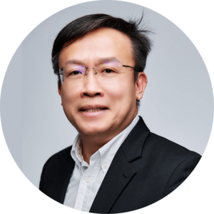
Dr. Choon Beng Sia
Test Technologist, FormFactor, Inc.
Dr Choon Beng Sia is a SSG Fellow, conferred by the President of the Republic of Singapore. He is also a Nanyang Research Scholar and has received doctorate degree in Electronics Engineering from Nanyang Technological University, Singapore. At MIT, Dr Sia studied data science and big data analytics.
In his current work at FormFactor as a Test Technologist in the Center of Expertise, Dr Sia develops and commercializes solutions to overcome emerging semiconductor wafer test and measurement challenges. His research interests include design, test and modelling of silicon-based RF devices, THz calibration and measurements for beyond 5G and IoT applications, photonics and power device wafer tests for LIDAR/Autonomous Transport/Optical communication applications as well as applying data analytics, deep learning and artificial intelligence to wafer tests and device modelling.
Dr Sia also serves in the IEEE MTT-3 technical committee that develops standards and best practices for RF measurements and he is also the MTT-3 speaker bureau specialising in wafer RF and 5G tests. Through SPRING, the Singapore National Standards board, Dr Sia represents Singapore as a Technical Expert in various IEC technical committees, developing standards for MEMs, optical and wafer-level reliability tests for semiconductor devices.
Dr Sia is a frequent invited speaker and organizer of IEEE workshops, international test forums and presently holds 12 international patents. Dr Sia has published more than 50 scientific journals and conference publications. His technical papers on RF, 5G production wafer tests and Silicon Photonics tests received multiple "Best Paper" awards at international wafer test conferences.
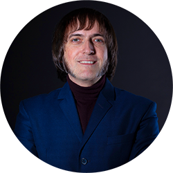
Bastian Tröger
Team leader of Product Management and Field Application, FRT Metrology / FormFactor, Inc.
As a graduate engineer specializing in physical optics, Bastian Troeger can look back on many years of professional experience in the area of optical metrology. His career at FRT started in 2007 in the development department, followed by the establishment of a new product management department and eventually led him to the management level of FormFactor FRT Metrology.

Amy Leong
SVP, Chief Commercial Officer, FormFactor, Inc.
Amy Leong has served as Senior VP, Chief Commercial Officer since January 2023, responsible for global customer sales and services, corporate marketing and M&A. From 2012 to 2022, she has held various management positions with FormFactor including Chief Marketing Officer and General Manager. Prior to FormFactor, Amy was VP of Marketing at MicroProbe from 2010 through the October 2012 closing of FormFactor’s acquisition of MicroProbe. Before joining MicroProbe, Amy worked at Gartner, Inc. as a Research Director from 2008 to 2010 and covered the foundry & logic market and various emerging applications. From 2003 to 2008, Amy worked at FormFactor where she served as Senior Director of Corporate Strategic Marketing and Director of DRAM Product Marketing. Prior to FormFactor, she worked in a variety of semiconductor process engineering, metrology, and product marketing roles at KLA and IBM. Amy currently serves as an independent board of director at Skywater Technology (NASDAQ: SKYT), the only US-investor owned pure-play semiconductor and technology foundry.
Amy holds an M.S. in Material Science and Engineering from Stanford University and a B.S. in Chemical Engineering from the University of California, Berkeley.

Bastian Tröger
Team leader of Product Management and Field Application, FRT Metrology / FormFactor, Inc.
As a graduate engineer specializing in physical optics, Bastian Troeger can look back on many years of professional experience in the area of optical metrology. His career at FRT started in 2007 in the development department, followed by the establishment of a new product management department and eventually led him to the management level of FormFactor FRT Metrology.

David Cooke
Sr. Product Marketing Manager, FormFactor, Inc.
David Cooke has a distinguished career in the semiconductor test and measurement community and with FormFactor. He has held positions in business development, account management and product marketing.
He has a masters of engineering from University of Massachusetts Lowell.

Simon Reissmann
Sr. Principal Applications Engineer, FormFactor, Inc.
Simon Reissmann holds a Bachelor and Masters degree in electrical engineering. He has industry experience in optical transceiver test and UV LED system from his previous employers Tektronix and Phoseon Technology. He currently supports silicon photonics customer outreach, testing and development for the FormFactor system business unit as Principal Applications Engineer in the Center of Expertise (COE).

Pratik Ghate
Principal RF Engineer, FormFactor, Inc.
Pratik Ghate received the B.E. (2014) in electronics engineering from Nagpur University, India, M.S. (2015) in electrical engineering from The University of Texas at El Paso, and Ph.D. (2021) in electrical engineering from The University of Texas at Arlington. His research interests include high frequency electromagnetics, RF design and measurements, antenna design and computational electromagnetics. Dr. Ghate joined FormFactor, Inc. in June 2021 where he is working as a Principal RF Engineer.

Hadi Najar
Sr Principal Engineer Mechanical Design, FormFactor, Inc.
Hadi Najar is currently Sr. Principal Engineer Mechanical Designer at FormFactor, Inc., Livermore, CA. He received his B.A.Sc. and M.A.Sc. degrees in electrical and computer engineering from the University of British Columbia, Vancouver, BC, Canada, in 2008 and 2010, respectively. He received his Ph.D. degree in electrical and mechanical engineering from the University of California at Davis (UC Davis), in 2014. His Ph.D. work and Post Doctoral Research focused on design and analysis of diamond-based MEMS resonators and hemispherical resonating gyroscopes. He was a Design Engineer with Texas Instruments, Inc., Santa Clara, CA in 2015. Dr. Najar has been the Chair of IEEE MEMS San Francisco-Bay Area chapter since 2016.

Jack De Grave
Director of Business Development, HPD / FormFactor, Inc.
Jack DeGrave joined the FormFactor-HPD Business Development team in early 2021 where he has focused on engaging with the Quantum Development Community members to map out the needs for cryogenic test and measurement, high density I/O device interfacing, and cryostats for deployment of quantum processors. His background in cryogenic test and measurement dates to early 2010 during his PhD studies in low temperature transport properties of helimagnets and skyrmions at the University of Wisconsin-Madison. After graduating, he held business development positions at several cryogenics companies. Jack brings greater than a decade of experience in cryogenic system design and test & measurement.

Dr. Deepak Kulkarni
FELLOW, ADVANCED PACKAGING, AMD
Keynote Presentation - Advanced Packaging: Enabling Moore’s Law’s Next Frontier
Chiplet architectures are fundamental to the continued economic viable growth of power efficient computing. Thus, the criticality of advanced packaging technologies and architectures correlated to Moore’s Law’s next frontier is high. New heterogeneous architectures, along with AMD’s industry leading advanced packaging roadmap, enable power, performance, area, and cost (PPAC). PPAC considerations per product influence the choice of Substrate (2D), Fanout based (2.5D) and Hybrid Bonded (3D) technologies and will be addressed in this keynote. Finally, AMD’s High Performance Fanout previewed in the RDNA3 architecture along with enabling technologies like power delivery and thermal improvements will be detailed.
Deepak Kulkarni is a Fellow, Advanced Packaging at AMD. Deepak has over 15 years of experience in packaging technology development. Over the years, he has held several leadership positions driving substrate technology development and yield improvement. Prior to joining AMD, Deepak was Senior Director of packaging yield at Intel Corporation. He holds eight patents and nineteen publications on various aspects of packaging such as 2.5D/3D architectures, DFM/DFY and AI techniques applied to yield management. His contributions to the semiconductor industry have been recognized by an Intel Achievement Award, Next 5% award (AMD) and best paper award (ITHERM). Deepak holds a PhD from the University of Illinois Urbana-Champaign with a major in mechanical engineering and a minor in computational science.

Pranav Shrivastava,
Principal Applications Engineer, FormFactor, Inc.
Pranav Kumar Shrivastava joined FormFactor GmbH Germany this year as a team member of CoE team at FFI. He done his B.Tech degree in Electronics and Communication Engineering from INDIA. Also completed M. Tech degree with the specialization in RF and Microwave Engineering from Indian Institute of Technology, Kharagpur, INDIA in 2014 and Ph.D. from Centre for Applied Research in Electronics, IIT Delhi, INDIA in 2022. His main research interests during his Ph.D. work involved RF micromachined components in mmWave range, phases shifters, RF MEMS switch, Sub-THz range metastructure and their characterization.
Presentation Video Request
Stay Informed
If you’d like to be informed when registration opens, please fill out this form. Your information will not be shared.
Questions or need help?

